Quantcast
Viewing all 71 articles
Browse latest View live

What the TTM/Viasystems Merger Means For the PCB Industry?

Now that two of the last big three (Sanmina being the third) circuit board manufacturers are merging, it has some wide ranging effects on the United States Printed Circuit Board industry.  To start, each merger of companies this size are priced to include “synergies” between the two companies.  The word synergy is code for closing facilities and cutting people to save money to pay for the acquisition.  This isn’t unique within the PCB industry, its common practice. TTM commented in their press release that they have identified $25 million in synergies that they will recognize in the first year.


TTM has 11 (7 domestic) facilities and Viasystems has 17 facilities (6 domestic) which will have to be rationalized. This is based upon the fact that very few of each of the company’s’ facilities are anywhere near capacity.  This puts some customers in a tough spot.  Do they wait to see if the facility that makes their products is closing or do they develop another source before then?  Once the facilities consolidate, will that effect lead times and the customers’ ability to expedite deliveries?  While public company mergers typically benefit shareholders, it puts additional stress on their customers.  Not to mention that they will need to deal with new customer service and sales personnel as the combined company needs to find those synergies.

Once the companies are combined, you will have an entity that generates 25% of their overall revenue from assembly operations. Viasystems had a substantial operation in China that did PCB assembly.  Most contract manufacturers in the U.S. don’t like to do business with companies that have competitive offerings. This makes another decision in which their customers must evaluate.

Effect on PCB Jobs and Education


In 1999 there were over 1,200 Printed Circuit Board shops in North America. With this merger and the subsequent facility closures, the number now may be just over 200.  This presents the employee’s and longtime PCB engineers with a significant challenge as there just isn’t a lot of PCB jobs left in the U.S.  Not only do we lose manufacturing capacity but we lose brain power that is used to research, develop, and test new technologies.  The lack of potential jobs also limits the number of young people who want to come into our industry which hurts our long term ability to innovate.

Decline of US PCB Industry Questions Small Shops


The PCB industry has been in decline for years in the United States. This is why the strongest companies in our industry have diversified to offer design services and other products that leverage the same strengths that create success in the circuit board space.  In addition the smaller PCB shops in the U.S. don’t have the resources either technically or financially to take on the higher tech work and its puts the customers in quite the conundrum.

Conclusion


Consolidation in various industries in the U.S. has created challenges and opportunities for both suppliers and customers.  The opportunity for suppliers who have been around for over 60 years like Epec is to demonstrate to customers how working with a financially stable, privately held company, with significant engineering, and manufacturing resources is a solid long term supply chain investment for their company.  Traditionally, larger companies viewed domestic suppliers as either too small or unsophisticated to manage their complex needs.  As the industry and the options for customers gets smaller, the best companies invest in their people and technology to fill that void.
How do you select the type of cell you would use in a battery pack?

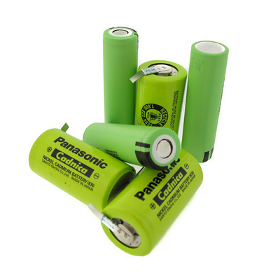
There are several factors when considering the type of cell to use in your battery pack design. Looking at the battery requirements and the dimensional space that is available are important. Another factor that comes up is pricing. The top tier manufacturer brands can be expensive but there are also Asia comparable solutions that will reduce the cost.

Occasionally customers have intentions to work with specific brand cells and models for their battery design. At Epec we have an extensive reputation and are partnered with some of the industry best cell manufacturers.  We are also assembly approved for the use of top tier brands such as Panasonic and A123.

Another important factor when choosing what cell to use for battery pack is the type of chemistry.  There are a number of different chemistries to consider for your battery pack design and all have different specifications and requirements. Our engineering team will work with you to determine the best battery chemistry selection for your application. 
Image may be NSFW.
Clik here to view.
Battery Cells
Battery Cells

More factors that may influence your decision when choosing the proper battery cell include: size, weight, form factor, power usage vs. energy usage, operating temperature ranges, cycle life, standby operation vs. cyclic operation, and cost vs. performance.

Once the application in which the battery pack will be used is fully understood, we can select the applicable chemistry that best suits your needs. Keep in mind that all these factors are all discussed up front when working with Epec’s engineering team to help develop a reliable custom battery pack for your end product.

Visit our website for more information on types of battery cell comparisons.


Use of Strain Relief with Rigid-Flex Printed Circuit Boards


With rigid-flex printed circuit boards (PCB’s), the transition from the rigid material to flex material (Transition Zone) can exhibit visual imperfections that, although acceptable, could affect the final part.

These imperfections can consist of adhesive squeeze-out, protruding dielectric materials, crazing, or haloing. With the protruding dielectric materials (resin), the particles can have sharp glass-like qualities.  If the parts are flexed at the interface, the remaining cured resin could damage the underlying flexible laminate.

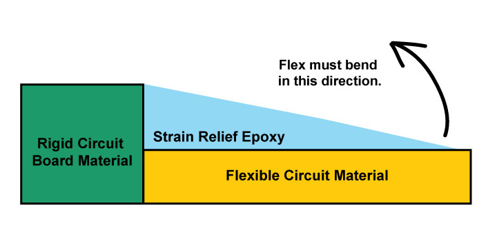
To protect the underlying flexible laminate, PCB designers will require a strain relief epoxy in the transition zone. This applied, cured epoxy will help to extend the bending area past the remaining cured resin. See below illustration.
Image may be NSFW.
Clik here to view.
Illustration of rigid-flex circuit board transition zone from rigid to flex material.

This strain relief epoxy can be controlled to be either rigid or flexible, depending on the requirements of the final product.

It is important to note that when designing strain relief into your rigid-flex PCB design that you should refer to IPC-2223, section 5.2.9 for guidelines and limitations.

If you have any questions or concerns with your rigid-flex board you can always reach out to us during the design stage, our engineers are always willing to help.  Be sure to download our flex and rigid-flex PCB design guide for additional information.

What It Takes To Be a Hybrid Supplier in the Electronics Industry

What Is A “Hybrid” Supplier?

Over the past several years, the term “hybrid supplier” has become more popular when describing companies that lead their industry in products and services.  The term “hybrid supplier” means combining multiple business elements with unique process to create a mixture.  A Hybrid Supplier is a company who combines the different business aspects to fill the customer needs under one company.  While this sounds like a very attractive business model for a customer to use, it is much harder than it sounds.

A hybrid supplier in the electronics industry acts as a manufacturer, distributor, and technical design firm for their customers.  The challenge for a company to truly be able to do this is that they need to invest significantly in becoming very good at each one of the three facets.  Taking the traditional PCB industry for an example, printed circuit board manufacturers’ who are no longer in business wanted to add distribution to their service portfolio.  The problem was that the same people were involved in both sides of the business, so which one took precedence?  Did anyone at the company truly know how to manage a global supply chain or was it just because they knew PCB’s and that would be enough?  In order to be a great hybrid supplier you must have dedicated and experienced people in every discipline of your business or you are nothing more than a low value add broker.

Image may be NSFW.
Clik here to view.
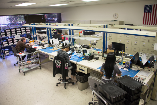
Epec's User Interface Engineering and Cable Assembly Facility in Largo FL


What Are the Key Factors for a Successful Hybrid Supplier:

1.    They Act Like A Manufacturer – AT ALL TIMES.

Most hybrid companies manufacture small portions of what they sell at facilities they own.  To do so they must invest in systems and people that allow them to respond and react like a manufacturer, even though they don’t own every factory.  It is far more than a vendor-customer relationship, and requires the same infrastructure as any manufacturing company.  The manufacturing company must be able to employ highly trained product experts, oversee production, engineer custom solutions, and have in-house quality teams at factory locations and in warehouses.  Additionally they must have the ability to manage and quickly address customer quality issues through their domestic resources and never have to wait to talk to a “vendor” to get an answer.

2.    Supply Chain Is A Core Competency.

Too many manufactures’ believe that product knowledge is the only expertise that a company needs to sell a product to customers.  Global Supply Chain management is much different than running a production facility. How can the same people do both?  Along with supply chain expertise - hybrid suppliers’ contract out manufacturing as needed to the manufacturer that they have approved for the specific type of product based upon the technology, delivery, and quantity.  Hybrid suppliers don’t get bogged down by force-fitting customers into their open factory capacity.  It may not be best equipped to manufacturer that product.  As a result, hybrid suppliers effectively have unlimited capacity and are not handcuffed to specific technology, quantity, or delivery.  On top of that, hybrid manufacturers with financial stability are able to hire supply chain professionals and allows them to manage inventory for customers helping their customers be more successful.

3.    REAL Investment in Technical Support for Their Customers.

Technical and design resources are key for the success of hybrid suppliers as they are basically an extension of their customers engineering department.  Traditional manufacturers and distributors have no problem making a product if they are given a perfect specification.  Hybrid suppliers on the other hand look to work with their customers at the development level to make a product more manufacturable and cost effective.  Whether it is full product design or supplying specific engineering resources, hybrid suppliers have the in-house staff required to provide customers with that level of service.  Hybrid suppliers realize the value in helping a customer get to market faster, with lower costs and the best quality product.

As more and more companies call themselves hybrid suppliers, customers need to do their homework to really understand if that supplier has invested in the three areas above.  It doesn’t need to be in-depth research; it can be something as small as if they manufacture products in China, do they have any employee’s in China?  Most companies don’t but they advertise themselves as being experts in China manufacturing but how so?  Some companies don’t even deem it important enough to invest in their own people within the facility when the factory is 8,000 miles away.

Conclusion

There are several companies in various industries that have invested and clearly have the right formula for success.   Even in an industry as competitive as packaging, Berlin Packaging of Chicago has revenues of over $800M by using this same strategy and executing it better than anyone else.  Hybrid Suppliers are the next evolution in numerous industries, but they require investment, dedication, and the financial resources to truly add value to their customer’s needs.

V-Scoring of Printed Circuit Boards in Arrays

 By Chris Perry, Quality Manager –  Epec Engineered Technologies

When designing PCB’s in a multi-up array, most designers choose v-score as the singulation method over traditional rout and breakaway tabs. The benefits gained range from effortless removal of parts from panel form, to realized cost savings with better utilization of panel area. When designing a circuit board with v-score, there are two areas of concern - the angle of the cut, and the depth of the cut.

Image may be NSFW.
Clik here to view.
V-scored PCB and a cross sectional view of a V-score cut.
V-Scored PCB and a Cross Sectional View of a V-Score Cut.

Referring to the angle of the cut, the wider the angle makes it easier for part removal. A narrow angle will leave a thinner channel, allowing the designer more flexibility with image placement. A 30° angle is standard, which leaves a .015” channel, but thicker materials such as .093” or higher, may be better suited for the wider 60° angle. The depth of v-score is measured by the remaining web thickness (groove center material left behind after v-score process). For standard laminates, at .062 thick, a .020” web thickness (+/-.004” tolerance) is recommended. For high temperature laminates, which tend to be brittle and fracture easily, a .015” web thickness (+/- .004” tolerance) is recommended for .062” thick laminates.

V-score does come with challenges. If the parts do not breakout easily, it can lead to fracturing of the circuit boards during singulation, and also part dimension issues. These issues can be caused by a poor singulation process, incorrect v-score specifications, or a quality shortfall at the actual v-score process.

Difficulty in breaking the parts from the v-scored array can be dependent on how the parts are removed from the array. In many cases manual hand separation is good enough to remove the assembled parts from the array. However, when the populated part leaves little room to sufficiently grasp the assembly, or the assembly uses a thicker laminate, a v-score cutter (pizza cutter) may be utilized. This cutter allows removal without unwarranted stress on the assembly itself.

When assemblies are difficult to remove, the forces placed on the assembly will cause what appears to be a haloing along the part edge. The haloing effect is a fracturing of the fiberglass bundles and resins of the base laminate. In a worst case scenario, the separation will happen outside of the v-score channel and cause uneven breaks along the board edge. Possible causes for this issue can be incorrect v-score depth specification for the laminate used or rough part removal, placing excess stresses on the part. Inconsistencies with the v-score itself can lead to this.  A dull blade or blades can cause the cut to be more of a “U” shape as opposed to the correct “V” shape.

Image may be NSFW.
Clik here to view.
PCB V-score Results with Dull Blade
PCB V-Score Results with Dull Blade

This will increase difficulty in breaking out and leave excess material after singulation.  An offset v-score - which is when one cut is deeper on one side of the part, due to blade settings, will also cause uneven and difficult singulation.

Image may be NSFW.
Clik here to view.
Printed Circuit Board Offset V-Score

Finally, we have seen some suppliers use a “milling” process or a controlled depth rout, as an attempt to replace actual v-score. When these parts are separated, there will be an excessive amount of material left over, that many CM’s and OEM’s will find problematic. This process is highly discouraged.

Image may be NSFW.
Clik here to view.
PCB Scored Edge with Mil Process

It is also important to note that with all v-score processes, there will be remaining laminate material on the part edge, after the parts are singulated.

Image may be NSFW.
Clik here to view.
PCB Scored Board Edge After Seperation

Typically the remaining material is too minute to affect the part fit, but if the design calls for a very low tolerance with unit fit, there could be an issue. Remember that if a part is scored on opposite edges, the remaining material on both sides can add up to enough that will cause a fit challenge in the final unit.

Make sure to download our Free Technical Engineering & Design Guides which are packed with data from our high tech manufacturing capabilities. 

Complex Wire Harnesses: Why Can’t They Be Fully Automated

A cable harness, which can be also known as a wire harness, cable assembly, wiring assembly, or wire loom, is a grouping of wires and/or cables that are used to transmit signals and to provide electrical power if needed. The wires and cables are joined together using straps, cable ties, cable lacing, tubing (either shrink tubing or non-shrink tubing), sleeving, electrical tape, conduit, braided extruded string, or any combination of these.

A cable harness is most commonly designed according to the geometric and electrical requirements of the ultimate piece of equipment it will be installed in.  A simple harness could consist of as few as three discreet components but they more typically include dozens of different wires and possibly hundreds of components. The wires and cables used to construct a wire harness are usually hook-up wires, coaxes, multi-pair cables, and multi-conductor cables.  A complex wire harness may include any combination of these various types of wires and cables, all dependent on the design of the harness.

Commonly Used in the Transportation Industry

The most common use of a harness is in the transportation industry, which would include automobiles, buses, trucks, planes, etc. Wire harnesses can also be found in construction machinery, industrial equipment, data communications related equipment, white goods, consumer products, or used inside box builds or any other electro-mechanical components.  A wire harness will simplify the manufacture of any of these products by integrating all the wiring into a single combination that allows for a drop-in installation.  For example, automobiles, buses, trucks, and planes have many components that require wires for them to perform.  All of these wires add up to miles in length.  A wire harness simplifies the installation of the wires by grouping the wires into a compact, simplified bundle that can be installed in one operation instead of running all of the individual wires – decreasing installation time.  By joining the wires, terminations, and other components into a harness, the components can be secured much more effectively against the effects of vibrations, abrasions, and in some instances moisture.  Using a wire harness will also optimize space inside of the larger component and decrease the risk of shorts during the initial install or during later field repairs.  Incorporating the use of flame retardant sleeves into the harness also aids in lowering the risk of electrical fires inside of the larger piece of equipment.

Image may be NSFW.
Clik here to view.
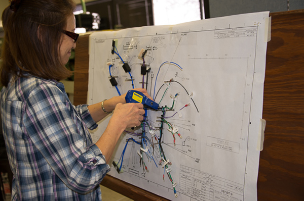
Wire Harness Assembly in Largo, FL
 Wire Harness Assembly in Largo, FL

Once the design of the wire harness is determined, a full size diagram is usually provided for the assembly preparation and assembly.  Based on this diagram, the wires are cut to desired lengths with the use of wire cutting machinery.  During the cutting phase the wire ends may also be stripped of insulation in preparation for further manufacturing steps.  The cut wires may also be printed at this stage for use identification in the overall harness, though in some instances the marking is completed during a separate operation.  With the ends of the wires exposed because of the stripping operation, they can now be attached to any required terminals or connectors.  Again the attachment of the terminals or connectors may be an automated process done on specialized equipment.   The terminated wires and cables are routed, assembled, and clamped together on a specialized workbench known as a pin board or assembly board.  This work bench is a full size layout of the wire harness and is built in accordance with the layout specifications detailed at the beginning phase of the wire harness design process.  The harness is also fitted with any ties, protective sleeves, conduit, or lacing at this point and when the harness is completed it is tested and shipped for inclusion into the larger equipment it was designed for.

In contrast to the trend of increasing automation, wire harnesses continue to be mainly manufactured by hand, due to the variety of different processes involved.  These processes include but are not limited to the following:
  • Installing terminated wires in varying lengths
  • Running wires and cables through sleeves and conduits
  • Taping the harness with fabric tape at branch outs
  • Conducting multiple crimps on specified wires (more than one wire into one terminal)
  • Binding the various components with tape, clamps, or cable ties
Because of the difficulty to automate these processes, manual production remains more cost effective than automation.

There are parts of the manufacture of a wire harness that can be automated however.  Automation can be effective in:
  • Cutting and stripping the ends of individual wires by using specialized cutting machines
  • Crimping terminals on one or both sides or the wires
  • Plugging of wires previously fitted with terminals into connector housings
  • Soldering or tinning of wire ends
The last phase of the manufacture of a wire harness is testing it for electrical functionality.  To partially automate this step in the process, a test board is typically designed.  The test board will have mating connections for each termination of the harness.  The harness will be “plugged” into the test board and checked electrically for any faults such as shorts or opens. 

Because of the lack of automation, wire harness production takes longer than other types of cable assemblies.  The entire process can run from a few days to several weeks, depending on the complexity of the harness – the more complex the harness typically the longer the production time.  

For additional information on cable assemblies visit our website and feel free to take a look at our cable assembly case study.

Lithium Battery Storage

 By Ed McMahon, CEO –  Epec Engineered Technologies

When you evaluate and examine the true stresses that lithium batteries encounter, most battery packs are designed to last three to five years if used and stored properly. Environmental conditions, not just charge cycling, are the key ingredients to longevity. The worst situation is keeping a fully charged battery at elevated temperatures. When not in use, batteries must be stored in a cool place. Most manufacturers will recommend storing at a 40% charge and being outside of the device it is used in. This allows for some self-discharge while still retaining sufficient charge to keep the protection circuit active.  Elevated temperatures and allowing the battery to sit at the maximum charge voltage for extended periods of time, is the most common reason for shorter than expected battery life. Additional stresses can even lead and nickel-based batteries.

Test data confirms that the best storage option of lithium batteries is if the cell is partially discharged. In one test by Cadex Electronics (http://www.buchmann.ca ) after 1 year in storage at 25°C the non-recoverable capacity remaining is 96%, when stored at 40% initial charge level, but only 80% if stored with 100% initial charge level. This effect is reduced at lower temperature and is a non-issue at 0°C but at higher temperatures the effect is much worse.

Image may be NSFW.
Clik here to view.
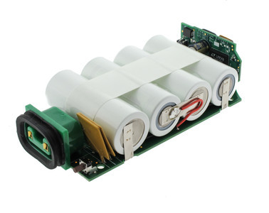
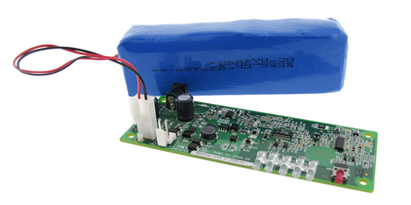
Lithium-ion Battery Pack with Sophisticated Control and Monitoring Electronics

If secondary cells or battery packs must be stored for a prolonged period the state of charge should be checked regularly and provision should be made for recharging the cells before the cell voltage drops below the recommended minimum after which the cells suffer irreparable deterioration. (This is particularly true for battery packs which may have associated electronics which add to the self-discharge drain on the cells)

Lithium-ion chemistry prefers partial discharge and since lithium-ion chemistry does not have a "memory", you do not harm the battery pack with a partial discharge. If the voltage of a lithium-ion cell drops below a certain level, it cannot be recovered.  This is also part of the reason that you want to use fuel gauge technology on all battery packs so that you can actively measure capacity and extend the life of the battery pack.

Also Lithium-ion batteries age, even if they are sitting on a shelf unused, and this capacity decrease is irreversible. So do not "avoid using" the battery with the thought that the battery pack will last five years. It won't. Also, if you are buying a new battery pack, you want to make sure it really is new. If it has been sitting on a shelf in the store for a year, it won't last very long. Manufacturing dates are important.

Interested in learning more? Check out the full battery pack development timeline.

User Interface Functional Test Schemes

By Paul E. Knupke –  Epec Engineered Technologies

This blog addresses custom user interface product testing prior to shipment. Generally, the first user interface assemblies shipment are for First Article acceptance testing where customers fully examine the first units for mechanical and electrical compliance to all engineering drawing and specifications. First Article inspection and verification occurs only once to qualify the first user interface assemblies. Unless design revision changes are requested by customers, electrical testing for future ship lots will consist of functional testing. The rational behind this approach is First Article or qualification testing addresses the product design plus manufacturing processes. Once the First Article unit is accepted, the qualification test of the design is complete.  Subsequent shipped User Interface assemblies do not require test to verify the design, only functional test is needed to assure the manufacturing processes and electrical functionality.

Custom User Interface functional tests are performed on each unit shipped by manufacturing personnel.  Additionally, final inspectors audit a sample of the ship lot quantity to confirm the functional test results.

Functional test schemes are divide into two user interface product groups. The first group is electromechanical user interface assemblies comprised of a matrix of switches and may include discrete LEDs individually connected or matrix connected. The second group is electronic user interface assemblies comprised of switches and may include discrete LEDs, digital or graphic displays, control electronics such as a microcontroller and active electronic interface such as USB or other serial protocol, or bus interface.


Electromechanical User Interface assemblies


Typically two identical commercial computer-based programmable test sets are used for functional test on user interface assemblies with switches and discrete LEDs. The test sets are programmed at the first use on a specific User Interface product.  Once the test program is verified, the program is stored electronically for future use.

The programmable test sets test all switches to verify open and closed resistance against thresholds, open and shorts in the User Interface circuitry, tests discrete LEDs by measuring forward voltage drop when illuminated and visual confirmation for proper color by the test operator. The collection of tests performed results in a PASS or FAIL indication with any deviation from test expectation classified as a test failure.  The test set provides the failure symptom on assemblies with a test failure.

Epec maintains an assortment of standard connector interfaces used between the assembly under test and the test set.  Occasionally, a new connector interface will have to be added when a new User Interface design uses an unusual I/O connector.


Electronic User Interface assemblies


User interfaces with active electronics between the assembly’s switches and the OEM’s application require a different functional test scheme.  In many cases, the functional test scheme will mimic the OEM’s electrical interface to the User Interface with additional test stimulation circuitry and a method of displaying test results.  Besides the physical electronic interface needed to connect to the User Interface, most electronic interfaces are encoded. For example, the test set must decode the data stream for an USB or other serial protocol to be useful for test purposes.
Image may be NSFW.
Clik here to view.
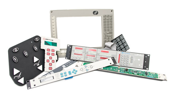
User Interfaces
User Interfaces

Development and custom built test sets that are unique to specific electronic user interfaces in a production environment can be created. However, developing and building a custom test set by the OEM may be a better solution. The OEM will be knowledgeable about the unique features needed in the test set because the OEM application will have the basis of the interface electronics already developed. All that is needed to complete the test set is a means to display individual test results for each switch function and a scheme to stimulate discrete LEDs or digital or graphic displays, if needed.  It is important to recognize that the test set should not duplicate the function or form of the end application. The test scheme needs to be geared toward production testing the User Interface, not the end application.  Close communication between Epec and OEM designers is needed to work out the most efficient and capable test scheme before the test set is fabricated.

If the OEM provides the test set hardware, it is further recommended that two identical test sets are fabricated – one for Epec to be used for final electrical functional test and one for the OEM to be used for verification test at receiving inspection. Experience shows that using two unrelated test schemes at both ends of the supply chain will cause future confusion if discrepancies are suspected. 


Other test set requirements


There are several other items concerning custom test sets that should be considered.  Test sets will be used in manufacturing and inspection departments by manufacturing and inspection staff.  The staff’s safety and conform should be considered during test as production testing can be tedious.  Little features such as the location and type of test controls as well as and positioning or holding the User Interface assembly under test will reduce the test staff’s fatigue.

A common mistake made by test technicians or engineers who design and build test sets is overlooking test connector wear and ultimate connector failure. Standard electrical connectors are designed for a specific use that includes a specified number of connection/disconnection cycles.  In an end application, a limited number of connector cycles before degrading or failure is rarely a concern.  In the test environment, the test set connector wear may quickly exceed the rated cycles on the connector based on the production rate.  The test set connector must be implemented in such a manner that the connector can be quickly changed when needed due to wear. A common solution involves a small test connector adapter cable or assembly. The adapter plugs between the User Interface assembly and the test set. When test connectors wear, the adapter can be simply unplugged and replaced to maintain test flow without interruption. Of course, replacement adapters must be maintained for this scheme to work.


Conclusion


Functionally tests on all user interfaces prior to shipment.  The style of test set depends on the complexity of the User Interface.  Early test planning during the User Interface design phase is needed to provide suitable and reliable functional testing when User Interface assemblies are first manufactured. Epec has the test experience and staff to handle customer’s functional test needs and can assist OEMs in understanding test techniques and their own receiving inspection test methods.

For full access to our User Interfaces - Technical Engineering Guide click the link.

Investment in Empowering Employees for Success

By Michelle Silva, Human Resource Specialist - Epec Engineered Technologies

At Epec, our staff members are our most valuable resource.  In this company, we celebrate each others success and support each others challenges. We strive to attract, hire, develop and retain passionate, talented, high performing individuals that are driven by our mission which is to provide a cost savings, technical resource and delivery advantage for our customers. We are committed to recruiting the best people that want to share our success, fit in our culture and live by our core values.

Image may be NSFW.
Clik here to view.
Epec's Core Values
Epec's Core Values


Some of the things that have been developing over the last few years to motivate employees include:

Training


Since 2013, there has been an investment in training employees. The focus of our training is advanced efficiency techniques and material flow optimization. This allows us more time to concentrate on marketing strategies to open doors such as new products and services for our customers while simultaneously providing our employees with enhanced and portable skills. It’s a win-win for both the company and our employees. By providing training opportunities, our employees become more productive and acquire new skills that affect the bottom line. Employees also have an opportunity to learn new skills, evolve within the company and develop professionally in their positions.
Recently in 2014, we introduced A3 training to our employees to engage in project work within their own areas of responsibility. Our focus in the A3 Process is to communicate problems, diagnose them and focus on solutions by laying out clear plans on how we are going to improve. Employees will be recognized for stepping up and executing great ideas.

Core Values


In 2014, there was an introduction to a set of Core Values. We have been working with employees to not only understand them, but live by them. Our Core Values are a resource to encourage employees to innovate, execute, and find a better, more efficient way of doing things. This transforms into getting work done right the first time around. Part of our core values includes making a difference, providing a positive experience, and creating bonds with our customers. This goes beyond being friendly; it’s listening, being helpful, and showing that we care about the concerns of our customers and going the extra mile.  There are weekly emails consistently to remind our employees of these values and how these values need to filter down to all teams so that their behavior and attitude reflect our values.

Rewarding Employees


For 2015, we have developed a new Performance Management Process which supports commitment to recruit, develop, and competitively compensate outstanding employees and to better prepare us to meet future. The objective of the performance process is to continue what should be an ongoing communication between employees and their supervisors so there is mutual understanding of responsibilities, expectations, and the details of the employee’s work. All while focusing on improvement, accomplishments, and future growth. Employees will be evaluated on more than just their job descriptions. They will be evaluated on how they are helping the organization achieve its goals. Communication and coaching to our employees from management is essential for employees to develop their knowledge and skills. We compliment as well as offer constructive criticism. Some of our goals for 2015 focus on customer service and response time, as well as, on-time delivery.


Polyimide Flex Core Material Types: Adhesive Based & Adhesive-less

 By Paul Tome, Product Manager Flex & Rigid Flex - Epec Engineered Technologies

Two distinct types of flex core material constructions are utilized in today’s flex circuit manufacturing.
The difference is in the method used to physically attach the copper layers to the polyimide core. This results in a different set of material properties for each of the material types which must be factored in to a specific application to ensure the design meets all the requirements and is cost effective.

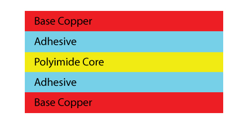
“Adhesive Based” flex cores utilize a layer of flexible adhesive to bond, under heat and pressure, each copper layer to the polyimide core. The adhesive is typically either epoxy or acrylic based and 0.0005” to 0.001” in thickness.
           
Image may be NSFW.
Clik here to view.
Adhesive Based Flex Cores
   
“Adhesiveless” flex cores have the copper directly attached to the polyimide core without the use of any adhesives.
Image may be NSFW.
Clik here to view.
Adhesiveless Flex Cores

 Adhesive Based Flex Core Benefits:  

  • Reduced Material Costs
  • Higher Copper Peel Strengths (Dependent Upon Adhesive Type Used)           


Adhesive-Less Flex Core Benefits:

  • Reduced Flex Thickness
    • Due to Elimination of Adhesive Layers
  • Improved Flexibility
    • Due to Reduced Finished Flex Thickness
  • Tighter Possible Minimum Bend Radius
    • Due to Reduced Finished Flex Thickness
  • Improved Plated Hole Reliability in Higher Layer Count Flex Designs (i.e. 3- 7 layer designs)
    • Reduces Number of Layers of Adhesive Within the Flex Construction
    • High Co-Efficient of Thermal Expansion of Flex Adhesives can Place Plated Holes Under an Excessive Z-Axis Stress During Assembly/Operation Which can Lead to Hole Plating Cracks
  • Higher Potential Temperature Ratings
    • Flex Adhesives have a Substantially Lower Max. Operating Temperature than Polyimide
  • Improved Controlled Impedance Signal Characteristics
    • Homogenous Construction of only Polyimide Between Signal Layers and Reference Planes.
  • Required to meet IPC 2223C Rigid Flex Design Guidelines
    • Eliminates and or Reduces the Use of Flex Adhesive within Rigid Areas
    • Improved Plated Hole Reliability
  • Better Suited to Harsh Environment Applications

Both material types are available with a range of Polyimide core thicknesses and copper weights. 0.001”and 0.002” are the most commonly used and cost effective core thicknesses. Thicker and thinner cores are available to meet unique specific design requirements. Thicker cores, greater than 0.002”, may be required for impedance controlled designs etc., but have a negative impact on flexibility, reliability and cost. Thinner cores, less than 0.001”, are available for very thin designs that require maximum flexibility but negatively impacts cost.

Both material types are also available with a range of copper thicknesses with ½ oz and 1 oz being the most common and cost effective. Thicker and thinner copper weights are again available to meet specific requirements. Thicker copper, greater than 1 oz, for higher current carrying requirements and thinner copper, less than ½ oz, for high circuit density and more flexible designs. Both negatively impact cost as compared to the ½ and 1 oz standards.

Which Flex core material type is best suited for an application? 

This depends upon many elements of a specific design. A full electrical and mechanical design review is recommended to ensure the design is optimized.

Please feel free to contact us if you have any questions or need assistance in selecting the correct material type for your design.


Why Disaster Recovery Planning Is Important For Any Business?

By Ed McMahon, CEO - Epec Engineered Technologies 

When we sat down in 2005 to develop our IT infrastructure plan for the company, I was a little unsure of why we spent so much time evaluating every investment in terms of what we would do in case of a disaster.  Well this winter, I found out why that was so important.  While not technically a disaster, New England had the most snow that we have had in over 20 years (with more to come it appears).

We’ve had 10 days where school was canceled and each time more than 5 inches of snow covered the roads making driving impassible. It was extremely important to keep our employees safe and not have them spend hours commuting 10-20 miles in their car trying to make it into work.  Before 2005, these issues would have caused our company to close down. This would mean that we would not be able to serve our customers in the way that they have come to expect.


Because our team spent so much time developing our disaster recovery plan we were able to operate at 100% capacity even though the snow kept on coming.  Some of the things that allowed us to continue operating included:

  • Having a cloud based ERP system and the balance of our IT infrastructure located at a secure offsite data center with backup power meant that we didn’t have to worry about our employees being able to get into our system and manage customer’s quotes, put in orders or get other information.
     
  • Our investment in our state of the art VOIP phone system allowed us to transfer our main incoming phone number to our location in Largo, Florida.  When the phone was answered in FL it was transferred back to the employee’s cell phone without the caller even knowing. This allowed many of our employees’ to work from home and be very productive.
     
  • 98% of our employees have company laptops enabling them to work remote. With a handful of state of emergencies declared over the past months, employees were able to work from home without the lack of resources.
     
  • Having such a deep relationship with UPS allowed us to work with them very early every day to best understand their plans.  Having a 5am call with the Regional Operations people gave us insight as to how to best plan our shipment schedule to meet customer requirements.  If we knew that they were going to be pulling their drivers off the road because of unsafe conditions we would make sure that our shipments were picked up well before that.

These are just a few of the things that allowed us to keep operating, along with the fact that because we have multiple locations in the US to provide backup if necessary.

Even though all of us living in New England have had enough of this snow, it’s reassuring to know that even in the worst conditions - our disaster recovery plan succeeded the disaster itself.


Dealing With Cable Assembly Obsolescence

One point that anyone involved with cable assemblies understands is that “every electronic or mechanical component will eventually reach the end of its life cycle”.  This blog post will define obsolescence as the point in an assembly’s life cycle when it is either no longer in a usable state, meaning it is not functioning as it was designed, or there is no longer a use for the cable assembly due to technology changes.

Obsolescence, or end of service life due to technology changes, is a very real issue in every industry including Datacom, Industrial, Medical, and Consumer products. Having assemblies that are performing the task that they were designed to do becoming obsolete due to technology advancements rather than reaching the end of its useful life is becoming quite common. In all industries the desire for the most advanced and up to date equipment is driving a very rapid development of new products.  In some industries, Standards Committees are developing interfaces that are replacing existing products and making those existing products obsolete years ahead of their expected end of life. Because of this transition to better technology, a designer needs to consider technology updates when designing a system and build assemblies accordingly.  If it is anticipated that a cable assembly will be outdated due to technology change in 5 years, it isn’t necessary to design and manufacture the assembly to last 15 years.

Image may be NSFW.
Clik here to view.
Quality Assurance Test for Cable Assemblies

Obsolescence, or end of service life due to a cable assembly reaching the end of its life cycle, is determined in large part by the design of the assembly, the materials used in the assembly, the construction of the assembly, and the level of workmanship that went into building the assembly in the first place.  When a cable assembly is being designed, the expected useable life of the assembly needs to be considered when choosing the raw materials to be used. 

Selection During Design Stage

In the design stage of an assembly, materials can be chosen that will determine how long of a useable life the assembly will have.  If the assembly is for an application that has a very limited or onetime use, materials are available that offer cost savings and are of a less durable nature.  At the other extreme, if an assembly is for a critical application or is expected to perform properly for many years, the selection of materials used in the assembly needs to be more critical.  For instance, in less critical applications a standard off-the-shelf copper conductor could be used as the transmission medium while in critical applications a copper alloy conductor with many very fine strands may be used.  By choosing copper alloy materials, the design engineer will develop an assembly that will provide a longer flex life and be more durable.   

Another decision to prevent premature obsolescence of an assembly due to failure is the choice of jacket materials. The material chosen for the jacket of an assembly will play a key role in the performance and useable life of that assembly. While the most obvious purpose of the assembly jacket is to make the assembly cosmetically attractive, the cable jacket also serves the purpose of mechanical, chemical, and environmental protection to the conductors within the jacket. The environment in which the assembly will be used will dictate the type of material the designer should choose for the jacket.  For instance PVC is a very good jacket material for most applications, but if an assembly will be exposed to a harsh environment the use of a TPR material maybe a better choice. 

Every cable assembly will use some form of connector that is made from injected molded parts.  As with jacket materials, there is a vast array of materials available for use in injection molding.  Determining the proper material exhibiting the properties most suitable for the application the assembly will be used in can be an engineering challenge.  Depending on the intended use of the assembly, a design engineer may choose materials that possess a high degree of impact strength or if the assembly will be exposed to cleaning solvents a material that is high in protection from liquids, oils, and gas could be used.  A designer should understand how the cable assembly or connector is to be used how long it is expected to last when choosing materials.

An additional issue that has an impact on the service life of an assembly is the way an assembly is manufactured.  Historically, cable assemblies fail at a much higher degree at the point where the conductors are terminated to the connector.  Manufacturing an assembly to avoid stress at the termination point increases service life and prolongs obsolescence.  Lowering or eliminating the stress at the termination point can be achieved through the use of a strain relief.  Almost all off-the-shelf connectors can be supplied with slip-on boots or strain reliefs.  The slip on strain relief does provide some level of relief, an over molded strain relief does a much better job.


Image may be NSFW.
Clik here to view.
Manufactured Cable Assemblies

Conclusion

For all users the critical question that needs to be answered when it is realized that obsolescence is about to take place or has already occurred, is what impact it will have on the business and what can be done to react.  With commercial components being declared obsolete at an increasing rate, the situation has become a major challenge for any company involved in the support of complex or long life equipment.

If obsolescence is predicted for the components used by a business, they should look at the following:
  • Use all existing stock that can be purchased through any source
  • Work with the manufacturer and utilize a “last time buy” philosophy
  • Institute a reclamation or cannibalization operation
  • Search for an equivalent which is functionally and technically interchangeable (form, fit, function, and finish)
  • Investigate any aftermarket suppliers of the item
  • Redesign the item that was designed out of the system

For additional information please fill out our Cable Assembly Information Request form.  

PCB Design: Solder Mask, Matte vs Gloss

By Chris Perry, Quality Manager –  Epec Engineered Technologies 

When designing a circuit board one factor that must be considered is the solder mask and whether to go with matte finish mask or gloss finish mask. Usually, most designers don’t specify which option and end up leaving the option to the PCB fabricator. This will likely lead to a gloss finishes which is more popular of the two.

A couple of questions to consider:
  • Should the designer be concerned with the mask finish?
  • What are the differences, and possible final results of the two mask finishes?

Image may be NSFW.
Clik here to view.
Solder Mask: Gloss & Matte
Printed Circuit Board Solder Mask: Gloss & Matte

There is no difference between the two types when discussing solder mask standards. Information on the use of solder mask is contained in IPC-SM-840C Qualification and Performance of Permanent Solder Mask. The specification is intended to facilitate evaluation of solder mask by a vendor using a standard board system, and to enable designer, manufacturer, and user together to qualify a production board process.
The prevalent difference between the two types is appearance. Gloss will be light reflective and lighter in color, whereas matte will have no shine and appear darker. Matte also tends to seem softer (porous) and gloss has a hard shell finish. In printed circuit board fabrication, there is no difference in the processes, and little difference in cost if any.

A matte finish may be more prone to scratching due to the softer finish, but scratches are more visible in gloss finishes.  Matte is also more likely to show surface cosmetics and white haze/residue. Gloss finish boards do not display this as much. However gloss solder mask can cause issues with vision systems at assembly due to its high reflectivity. Mask clearances around fiducials play an important role with vision systems, when using gloss finish mask.

There are many reports from Contract Manufacturers (CM) that matte finish is less susceptible to solder ball formation. When questioned, CM’s will rank the mask type as the #1 reason for solder ball formation with flux type also playing a major factor. There are several causes that result in solder balls. They are usually present on the bottom side of printed circuit boards. It has been the increase of the use of no clean low residue soldering that has focused more attention on the problem.

Why does matte seem to perform better minimal solder ball formation?


Over the years a number of possible reasons have been proposed behind solder ball formation. Some of these reasons include: solder mask glass transition temperature, solder mask surface energy, solder mask hardness, flux types, the presence of moisture, and solder mask surface roughness to name a few. To date, the exact mechanism is still not fully understood although surface roughness has always been a major factor in solder ball generation.  A technical report from Vantico (formerly Ciba Specialty Chemicals), showed that molten solder on a rough (matte) surface behaves differently than molten solder on a smooth surface -- for a variety of solder masks, and laminates.  On a rough surface, the molten solder forms a convex meniscus, and on a smooth surface the molten solder forms a concave meniscus.  The convex vs. concave meniscus reduces the area of solder ball attachment, so solder balls do not adhere as well to a matte surface as a smooth surface.

There have been numerous studies performed on solder mask “gloss levels” and the correlation with soldering defects. Photo imaged solder mask gloss levels were found to affect the number of solder defects created during the circuit board wave soldering process.  These solder defects (solder balls, solder shorts, solder bridges) were proportional to the solder mask gloss level. As the solder mask gloss level is reduced, the level of solder balls is reduced at a faster rate than the number of solder shorts and bridges. In other words, to reduce or eliminate solder shorting, the required gloss level is lower than required to reduce solder balls.

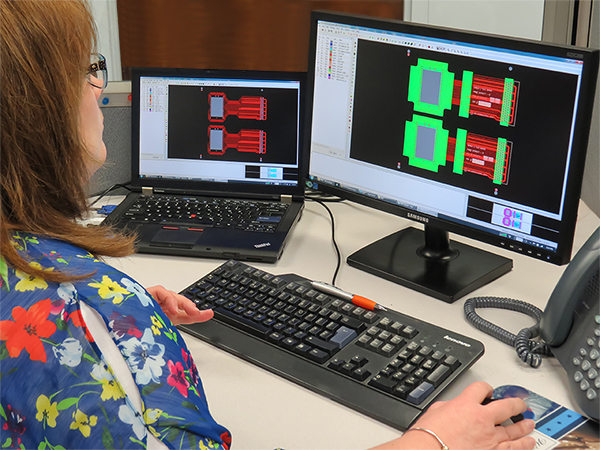
Engineering From A Woman's Perspective

By Sherry Clowers, CAM Engineer –  Epec Engineered Technologies  

Image may be NSFW.
Clik here to view.
Sherry Clowers
Engineering in most industries, still tends to be primarily dominated by males.  When I first entered the field of Printed Circuit Board (PCB) Engineering, it was a bit intimidating. This was because the men always outnumbered the women.  I felt we were graded on separate standards “Men vs Women”.  When I think “engineer”, I think of the really smart people, the designers, creators, and problem solvers. It is such a prestigious title and it is an honor to be a part of the Engineering Industry.  In the PCB field a woman’s job was typically restricted to Quality Control (QC), print, testing, and customer service positions.

For years I had been working in other areas of the industry earning the respect of my peers, but now here I was feeling a little isolated and feeling like I was starting all over again.  At first it was a struggle.  There were many times I wanted to give up – to just throw in the towel because I didn’t think I had what it took to be an engineer.  The pressure to succeed was often followed with sleepless nights.  Deciding to become an engineer was not something I had dreamt up during my childhood.  Printed circuit board manufacturing wasn’t even in the plan regarding the occupation I would enter.  It began when a friend of mine introduced me to her boss who happened to work in the PCB manufacturing field. At the time I had no experience in the work force; sheer determination drove me to succeed.  After working in several areas of manufacturing, I began to notice the details that went into the process of a PCB board.  Working hands on I was able to see the full scope of engineering circuit boards.  After working within the industry for three years, I was given a position as a CAD operator.


The men eventually noticed I could hold my own and wasn’t one to hinder. It was clear I was an asset to the team and in turn I was naturally accepted.  To my surprise it wasn’t just the men that I had to deal with along the way, but women as well.  You would think as a woman entering a field such as this, there would be a sort of “sisterhood” where women would try to do everything possible to help one another. However woman can equally be involved in confrontation, there are always a few who feel the necessity. However in the end it all worked out for the better.

I am so thankful that I was given the opportunity to work at Epec Engineered Technologies.  The Engineering Team embraced me before they even knew me.  They were not afraid to share their knowledge, they understood as a team if one of us succeeds, we all succeed and benefit from it.  Epec has one of the best, most knowledgeable, and caring engineering teams I have ever worked with and it is my pleasure to be a part of it.  Working with Epec makes my job more enjoyable and when you enjoy your job you are determined to excel.

To learn more please visit our website www.epectec.com.

Insuring a Proper Battery and Charger Match

By Battery Engineering Team –  Epec Engineered Technologies   

In today's battery and charger market companies may provide either battery assemblies or battery chargers, but few provide both. In the past buying a battery from one source and a charger from another worked just fine when using the older NiCd batteries with overnight chargers. However, with today’s new battery chemistries and the increasing need for faster charge times, careful matching of the charger to the battery is essential. Without proper matching, safety, cycle life, or run-time may be greatly affected.

Fast-charging NiCd batteries at rates of 1C to 4C, safety can be an issue. In these high-current applications, battery temperature must be monitored electronically, so precise control of the charger can be obtained. Once the battery is fully charged, the high-charge rate must be reduced to prevent the battery from going into thermal runaway and venting.
Image may be NSFW.
Clik here to view.
Lithium Polymer Pack & Custom Charger

Charger Impact on Battery Cycle Life

Cycle life can be impacted by treating batteries from different battery manufacturers in the same manner. While there are numerous manufacturers providing Li-lon and NiMH batteries, this doesn’t mean they should all be treated the same way. Inspection of the manufacturer's data sheet revealed that some types of NiMH batteries can take a continuous C/1O overcharge, while the most popular types of NiMH batteries cannot take this type of overcharge without severely affecting the cycle life of the battery. Precaution must be taken to understand the difference between the various manufacturers of Li-Ion batteries and how these differences affect the charging characteristics of their batteries. Some manufacturers require 4.1Vlcell charge voltage while others require 4.15 V/cell or 4.2 V/cell charge. If these voltages are exceeded by as much as 50mV, the battery will overcharge affecting the cycle life of the battery and causing safety issues.

Insufficient Battery Run Times

Insufficient run time is caused by undercharging the battery, which can happen by misapplying technology. An example would be the charging of a 4.2 V/cell Li-Ion battery using a 4.1 V/cell Li-Ion charger or by not fully characterizing the system dynamics. Some early termination problems can be caused by system noise by operating outside the temperature range of the battery or by using a mismatched thermistor in the battery pack. The only way to insure the battery and charger are matched correctly is to buy the whole unit from one source that has the expertise in designing and providing fully custom battery assemblies and fully custom chargers to meet the requirements of the customer.

Sourcing a Complete Battery, Charger, and Power Solutions

This "one stop shop" approach to battery and chargers can be extremely beneficial to the source purchasing the batteries and chargers. Primarily, if the battery and charger are ordered from two different sources, the customer will need to coordinate the design of both the battery and charger. This may require the customer to have expertise on batteries, chargers, and inherent safety devices. This is especially true in the newer Li-Ion or NiMH technologies are implemented using a fast charger and fuel-gauge. If the overall battery and charger system does not work, who will take the blame? Ultimately, it will be the responsibility of the customer to determine if the battery or charger or both are at fault. Since the two sources that provided the equipment may be reluctant to change their designs, the intervention of a third engineering party may be required. This can prove costly. By using a source that specializes in providing complete battery, charger, and power solutions, the customer only needs to provide the overall system performance requirements, and the engineers at the "one-stop shop" will work out all the engineering details.

The end result is improved time-to-market, reduced development cost, and a finely tuned battery and charger system. The ultimate benefit is that the customer can concentrate on their core competency, which will ultimately affect the competitiveness of their end product in the marketplace.

Feel free to visit our Battery Pack Development Timeline for additional information on process expectancy. 


Packaging For User Interface Assemblies

By Paul E. Knupke –  Epec Engineered Technologies

Packaging for shipment to customers is the last step in the manufacturing process.  Epec pays as much attention to packaging detail as to design and manufacturing of custom user interface assemblies.  Each custom assembly part number is by nature different size, mass, and shape because it is custom.  However, styles of User Interface assemblies can be grouped in several categories.  Experience has shown the type of packaging that works best is based on complexity of construction, shape, size, mass and shipped unit volume. No one packaging solution works for every assembly style.

Static Sensitive User Interface Assemblies

All assemblies that are classified as static-sensitive (includes electronic components) must be packaged in conductive bags and the mouth of the bag folded and sealed with an ESD (Electro Static Discharge) warning label.  Conductive bags must be conductive, not ant-static pink poly bags. The pink poly bags do not generate static changes but do not protect against ESD. 

Once the static-sensitive assemblies are protected from ESD and electrical damage, the assembly must be protected from mechanical damage during shipment. User Interface assemblies that are small mass and not static sensitive will be packaged in bubble bags. User Interface assemblies that are classified as not being static sensitive contain a matrix of switches and non-electronic components. Larger assemblies that are not static sensitive will be protected with bubble wrap.
Image may be NSFW.
Clik here to view.
Individual Packaged Static Sensitive Electronic Components

Some very large or critical-application User Interface assemblies are best packaged in unit boxes inside master boxes. User Interface assemblies may contain shape corners on rack panel or printed circuit boards, long threaded exposed studs, protruding hardware or exposed connector pins without a connector shoulder. Special packaging protection must be designed for these assemblies as needed. 

Custom Packaging Schemes

Once the packaging scheme has been determined for the custom user interface assembly, the packaging instructions and packaging materials necessary are documented in detail and added to the engineering drawing package for that custom User Interface assembly part number.  Adding the packaging information to the drawing package and Bill of Material and has several important advantages:

  • Packaging will be consistent for each shipment and will not depend on the staff’s memory from shipment to shipment.
  • Packaging will be planned and ordered when the User Interface assembly’s material is ordered from the BOM so that the proper packaging will be available at the time of shipment.
  • Packaging inspection is performed by the Quality inspectors as part of final inspection process to insure that the packaging instructions and materials are used as documented.

Some User Interface assemblies are built on a 19 inch rack panel as the mechanical base using both front and rear panel sides for mounting the components of the assembly.  A practical approach for protecting these assemblies is suspending the assemblies with rack panels in custom slotted EthafoamTM* spacers.  The exposed mounting ends of the rack panels are slid into the slotted spacers.  Slot spacing determines the space between adjoining assemblies. This packaging scheme prevents individual assemblies from contacting other assemblies or exterior walls of the shipping box.  Less packaging protection is needed on the individual assemblies because nothing touches the front or rear of the assembly.  For static sensitive assemblies using rack panels, assemblies will be placed in conductive bags and then slid into the foam slots. One of the benefits of this packaging scheme is the unit count is consistent in each box making count verification easy at both ends of the supply chain.  Individual panels can be easily slide out from the slots for inspection and reinserted without other assemblies falling together in the shipping box. Labor is greatly reduced for both packing at Epec as well as unpacking at the OEM.
Image may be NSFW.
Clik here to view.
User Interface with Front and Rear Mounted Components

Still other packaging options are used by Epec. One option is “egg-crate” cardboard inserts to create partitions in shipping boxes for some User Interface assemblies.  Another option is convoluted foam mounted to folding cardboard that slides into cardboard sleeve or inserts into a cardboard box to protect assemblies.

Conclusion

For each custom User Interface assembly, manufacturing designers determine the best packaging solution for each custom assembly that addresses factors such as protection level, ease of inserting and removal from a larger shipping box, ease of count verification, minimized packaging weight and cost. Packaging documentation and inspection insures consistency and protection for each shipment.


*EthafoamTMis a Trademark of Dow Chemical Corporation

Controlling PCB Costs: Part 1

Avoiding Expensive Materials And Processes

 By Al Wright, PCB Field Applications Engineer –  Epec Engineered Technologies

Printed circuit boards are just one component in an assembly which needs to be designed for the best cost-to-performance ratio possible. The finished product in which the PCB is installed must meet a price point that compares favorably against competing products. In order to make the best choices during the design cycle, it is important to first understand what some of the cost factors are. Once you understand which factors add cost, you will be to design your PCB to perform as required, without making the circuit board more expensive than it needs to be. The following is an explanation of some common cost drivers and some suggestions for how to avoid incorporating them in your design.

PCB Laminate Selection - Don't Skimp, But Do Not Over-Spec

Selecting the appropriate printed circuit board laminate is the first step, and there are many things to consider. Generally speaking, start by selecting a material which meets your requirements for electrical and thermal performance. For instance, if you have controlled impedance requirements, then you will need to consider Dk and Loss Tangent specifications. If you will be employing multiple assembly cycles (2-sided SMT assembly, for example) then pay attention to thermal performance, such as Tg, Td, and CTE. At all times keep in mind the surface finish you will be using. Higher soldering temperatures are required for lead-free finishes will put greater thermal demands on your material.

Your goal should be to meet or exceed all performance requirements but not to pay extra for requirements you don’t really need.  If your design is a 4-layer, power/ground PCB with SMT components on only one side, you may not need to give as much weight to the CTE as you would for a 12-layer PCB with 2 sides SMT, BGAs, etc.

Whenever possible, specify your material to industry standards. The best way to proceed is to familiarize yourself with the materials as defined in IPC4101C and to call out the laminate by the “slash number” for the set of specifications that will meet your needs. As a starting point, all fabricators will stock materials that meet 4101C/21, /24, /26, and to an increasing extent, /126.

One final word: Be sure not to go overboard trying to save cost. Skimping on material at the front end can cause costly failures at assembly, or later in the field, where the added value will far exceed the cost of using what would have been the appropriate laminate for the bare circuit board.

Avoid Excessive Blind and Buried Vias

Image may be NSFW.
Clik here to view.
Here is a typical cross-section for a 12-layer PCB with a total of 4 drill cycles and 2 laminations.

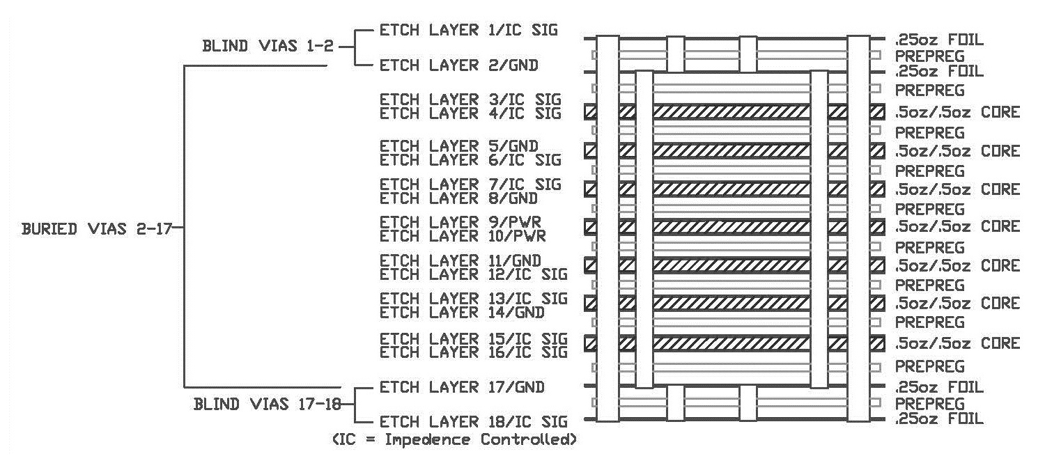
Minimize the number of extra drill and lamination cycles whenever possible. Try not to exceed 4 drill cycles (2x blind, 1x buried, 1x through all.) Here is a typical cross-section for a 18-layer PCB with a total of 4 drill cycles and 2 laminations. This requires only 1 more lamination step than a standard multilayer, and the drilling is balanced about the centerline.

Printed circuit boards are getting smaller and smaller, and it is necessary to use every little bit of space to form interconnections. This trend drives an increase in the need for blind and buried via drilling, which in turn requires sequential lamination (meaning that the PCB must undergo multiple lamination cycles so that each set of drilled holes can be drilled, plated, and processed before all of the sub-laminations are put together.) The combination of blind and buried drilling with multiple lamination cycles is called High Density Interconnect (HDI) processing.

HDI processing is practically routine when it is well-designed, but it remains expensive, and a poorly-planned HDI design can be difficult or even impossible to produce. We once received an RFQ submission for a very simple, low-density 10-layer PCB with 7 different drill cycles. That printed circuit board was literally impossible to manufacture, and our only choice initially was to no-bid it. We did provide some suggestions, which helped the customer to re-think his design, and to come up with something more workable.

When designing an HDI PCB, try to limit blind drilling to the top and bottom layer, connecting to the immediately adjacent layers, while limiting buried vias to a single pass which connects the two outermost internal layers. For example, a 12-layer with blind vias from 1-2 and 12-11, and buried vias from 2-11, only adds one extra lamination and HDI processing cycle. While this will not cover every eventuality, it is an ideal configuration for manufacturing.

If you initially find yourself needing a large number of blind and buried layer interconnections, look for ways to simplify. The fewer lamination cycles are necessary, the less your PCB will cost. The customer above, who started out with 7 drill files, eventually managed to make all of his interconnections using only through vias, without resorting to any HDI processing at all.

Inefficient Machining

When drilling or routing circuit boards, fabricators typically improve throughput by stacking the material so that multiple sheets may be processed simultaneously .062-thick PCBs are most commonly drilled in a 3-high stack, and under certain circumstances even 4-high is possible. The stack height is mainly determined by the diameter of the smallest drilled hole, which has been shrinking steadily because of the ever-smaller via diameters required as PCBs become smaller and smaller. Use of materials thicker than .062 also affects stack height.

Image may be NSFW.
Clik here to view.
CNC Machines
CNC Machines typically employ three or more spindles for drilling and routing. The more panels for fabricator is able to stack under each spindle, the more economical these processes become.

With miniaturization driving PCB designs towards higher density, it is pointless to recommend that all vias be specified at, say, .028 diameter, so they can be drilled in a 3-high stack. Nonetheless, if it is possible to use vias that are .015 or .018 diameter, instead of .010, and if doing so will not either create spacing problems, or drive you to a higher layer count, then consider using the larger size. Doing so will allow for 2-high drilling, which will cut drilling time for your order in half compared to a design that uses .010 or .008 vias.

The same goes for routing. Routing cost drivers include small slot widths, small minimum inside corner radii, and small channel size on routed sub-panels. Slot or channel widths below .062, and inside radii below .031, will reduce your fabricator’s stack height from three to two. Below .047 width and .023 radius, the stack height drops again, to one. Avoid cuts that require small-diameter routing burrs whenever possible, and consider drilling relief holes at inside corner locations, in place of small radii, when a flush fit is required. Routing is one of the final steps before shipping; an overly long cycle time draws a lot of attention, and adds cost to your order.

Conclusion

Lamination, drilling, and routing are all bottleneck departments in the PCB production cycle. Awareness of cost adders related to these processes will help you to make informed choices about which design features are necessary, and to modify or eliminate those which are not. The result will be a reliable product, at the best possible price.


Epec Donates to American Heart Association in Support of Employee

By Keith Araujo, Marketing Manager

This blog post is not the usual topic you find on Epec’s company blog.  We are normally blogging about technology solutions focusing on issues that can help our customers, but as a company, Epec does a lot behind the scenes for their employees that go unnoticed.

This topic is one that touches close to my heart, no pun intended. My beautiful daughter Keiana was born in early 2015 with a congenital heart defect called Tetralogy of Fallot (TOF).  Her condition was originally detected as a heart murmur, but after additional testing it was diagnosed as TOF.  We were told that her condition required her to have open heart surgery to repair the defect. This past April, at 3 months and 8 days old she underwent surgery at Boston Children’s Hospital. She is now 5 months old and is doing great!

During our stay at the Boston Children’s Hospital we saw many families from all walks of life. At that moment my wife and I decided that we wanted to give back to organizations that support cardiac research that might someday help save life of another child.

So what did we do? We started “Team Keiana” and joined the Southern New England Heart Walk to help raise awareness and funds.  Once Ed McMahon CEO of Epec, heard the news, he announced that Epec will match all donations made to the American Heart Association by their employees.
Image may be NSFW.
Clik here to view.
Epec Donates to American Heart Association in Support of Employee

A simple email went out to all our US employees 5 days before the race, within minutes to donations started coming in.  In just 2 ½ business days Epec’s employees donated $650 dollars, which was matched by Epec for a total of $1,300.

As a manufacturer of custom build to print electronics, Epec also works with several internationally known medical device manufacturers. In part, Epec has deep ties into the medical devices that are used to save lives every day.

I would like to conclude this post by saying thank you to everyone in our Epec family for helping with this great cause.

Thanks for the support…
~ Keith Araujo


Controlling PCB Costs: Part 2

LAMINATE UTILIZATION - PART AND PANEL SIZE:

By Al Wright, PCB Field Applications Engineer –  Epec Engineered Technologies

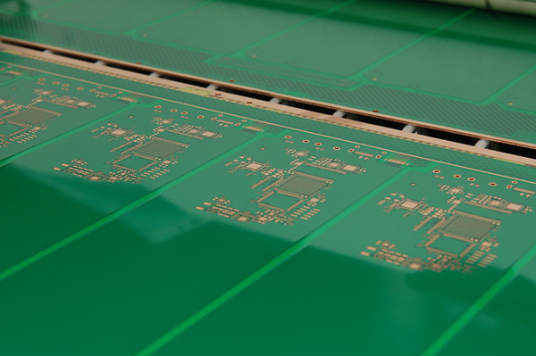
Printed circuit boards are run through the fabrication process in sheet form, typically with rows and columns of identical circuit boards or sub-panels on a single sheet, which are later cut out for shipment. One of the biggest potential cost adders in PCB manufacturing is that of a poor-yielding PCB or sub-panel. While this is true for even the least complex PCBs, it is especially true for multilayers.

The reason is that multilayers must be laminated in a thermal press near the beginning of the production cycle. There is only so much capacity available, and cycle times cannot be rushed. The efficient use of sheet stock is therefore a big factor in preventing bottlenecks at this critical production stage.

As an example, if your fabricator can only fit two printed circuit boards per press cycle versus four printed circuit boards, your order will obviously take twice as long to move through lamination. Aside from the up-front negative impact of the cost adder, this means a quick turn may not get through on schedule, or a large order may consume several shifts of lamination time before it can be drilled. To avoid creating such costly bottleneck situations, pay close attention to the size of both your PCB and your sub-panel.
Image may be NSFW.
Clik here to view.
Good-Yielding Sub-Panels for 18X24 Sheet Stock

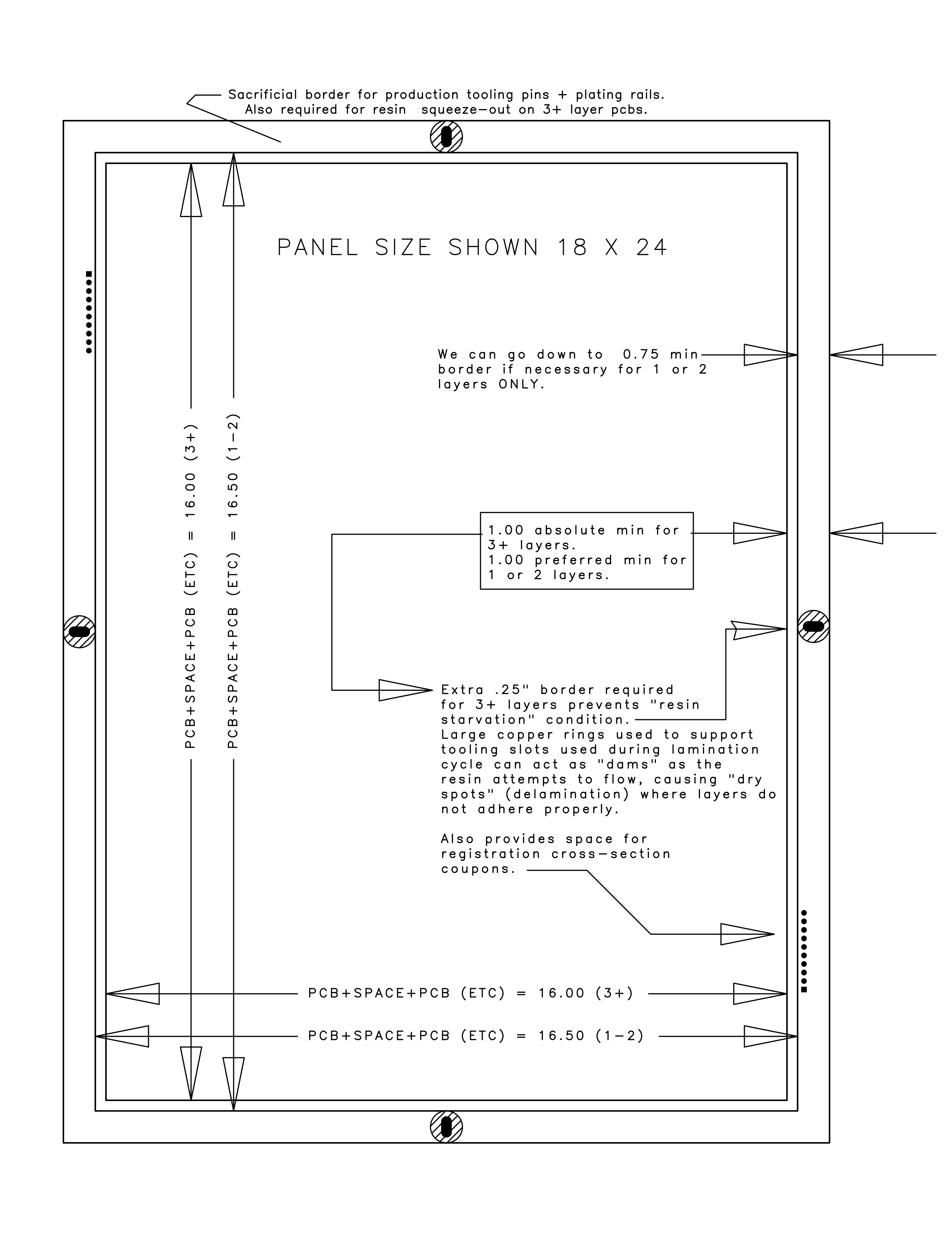
It helps to understand that most fabricators use machined metal plates in their lamination process. These plates are very costly, so typically a fabricator will stock just one or two standard sizes. In the USA, the most common size by far is 18x24, with some also employing 16x21 or 12x18 plates. You need to understand that whatever size PCB or sub-panel your fabricator will be shipping to you must make efficient use of material in this size.

Be aware also that the edges of the process sheet need to be left free of PCBs, because they must be used for locating fabricator tooling hole patterns, test coupons, plating rails, etc. At the interior of the sheet,circuit boards which are not v-scored require that space be allocated for routing channels required to form the edges. It is therefore not a simple matter of creating a unit size that divides evenly into an 18x24 sheet. To more fully understand process sheet utilization, please refer to the included diagram.
Image may be NSFW.
Clik here to view.
18X24 Diagram with Margins Required for Processing

For more information on PCBs please visit our main printed circuit board page for more information. If you're looking for design help on your current circuit board project or want to learn more our engineering team can help.


How Cable Assemblies Are Tested After Manufacturing

By Brian Morissette, Cable Assembly Product Manager –  Epec Engineered Technologies   

One of the most critical elements of producing a cable assembly or harness is the amount of testing that is done on the assembly/harness when it is completed in manufacturing.  There are numerous levels of testing that can be done, but all of the testing has one goal in mind – to ensure that the assembly/harness will meet or exceed the specifications it was produced to. For the discussions of this article, the mentioning of an assembly will mean both a cable assembly and a wire harness.   

Cable assemblies can be built to one or many specifications. For example, an assembly may be produced to a customer specification with regards to the color of the jacket and over mold material used, among other customer centric requirements, but from an electrical standpoint the assembly may be required to meet an industry standard.  Based on the specifications and standards the assembly was produced to, a final test plan is constructed that the assembly will be tested to. The test plan states the pass/fail criteria and the assembly is deemed serviceable if it meets, at a minimum, the pass criteria. 

At a bare minimum, cable assemblies need to be tested 100% electrically for shorts, opens, or incorrect wiring.  The proper method to electrically test an assembly is to attach the connector at each end of the assembly to a mating connector.  The mating connector will be attached to a fixture that will check for opens in the assembly, shorts between the conductors or the conductors and shields if any are present, and the proper pin placement for all the components of the assembly.  This setup puts the assembly into a test situation that fully replicates the installation that the assembly was built for. 

Additional testing may be considered from a visual, environmental, mechanical, and signal integrity standpoint.  The use of EIA Standard 364, IPC/WHMA-A-620B, and any other relevant industry standards documents should be used as guidelines for this testing.  These additional tests may not be necessary on all assemblies and the below information is presented as guidelines to consider:

Image may be NSFW.
Clik here to view.
Cable Assembly Signal Integrity Analysis

Visual

  • The connectors and/or sockets will be inspected to assess workmanship, proper markings, correct finish, appropriate materials, and design and construction.  
  • The entire assembly will be inspected dimensional to ensure compliance to the specification it was built to. The visual inspection will also check for any defects present such as deformation or blistering of the outer covering of the cable or the connector.

Environmental

  • High Temperature Aging – The assembly will be subjected to an elevated temperature to see what impact it will have on either the electrical or mechanical attributes of the connectors or cable used in the assembly.
  • Low Temperature Aging - The assembly will be subjected to a decreased temperature to see what impact it will have on either the electrical or mechanical attributes of the connectors or cable used in the assembly.
  • Thermal Shock/Thermal Cycling – The assembly will be subjected to high and low temperatures to evaluate what impact the temperature fluctuation will have on the connectors, cable, and termination points.
  • Humidity – The assembly will be exposed to high levels of humidity to evaluate what effect the raised humidity will have of the connector, cable, or termination points
  • Salt Spray - The assembly is exposed to a salt spray or fog to check for corrosion resistance of the materials and coatings used in the construction of both the connectors and the cable.
  • Vibration Testing – The assembly is subjected to repeated and constant vibration to evaluate the impact on the connector interface and the terminations.
  • Industrial Corrosion – The assembly is exposed to different climates as a method of accelerating in use corrosion failures to estimate service life of the assembly.

Mechanical

  • Mating and Unmating – The connectors will be mated and unmated to determine the force needed to engage and disengage the assembly.
  • Durability – The assembly will be subjected to repeated flexing at a set angle for a set number of repetitions determining the approximate life expectancy of the assembly.

Signal Integrity

  • Eye Diagram Analysis – Data eye diagrams are used in high speed signal analysis to show the key parameters of the electrical quality of a signal by using bit error testing. 
  • Time Domain Measurements – Time domain measurements will test the assembly for Intra-pair skew, inter-pair skew, and differential impedance
  • Frequency domain measurements – Frequency domain measurements will test the assembly for far end crosstalk and attenuation
  • Insertion Loss – The assembly will be tested for a loss in signal power which results from the inclusion of a component into the circuit.  The components typically inserted into the circuit would be connectors, splices, or filters. 
The above list is by no means meant to be totally inclusive of the testing that is to be considered for cable assemblies.  Additional testing such as insulation resistance tests, Hi-Pot testing, Safety certifications, and numerous other customer and industry requirements should be considered as potential testing areas. 

In summary, cable assemblies and cable harnesses should be produced by reputable manufacturers that have the means to do a complete testing plan and perform the tests documented in the plan. For us to begin working our your cable project, fill out this form.      
   
Viewing all 71 articles
Browse latest View live